- 您现在的位置:买卖IC网 > Sheet目录2003 > LTC1099ACN#PBF (Linear Technology)IC A/D CONV 8BIT HI-SPEED 20-DIP
LTC1099
7
FUNCTIONAL DESCRIPTIO
UU
U
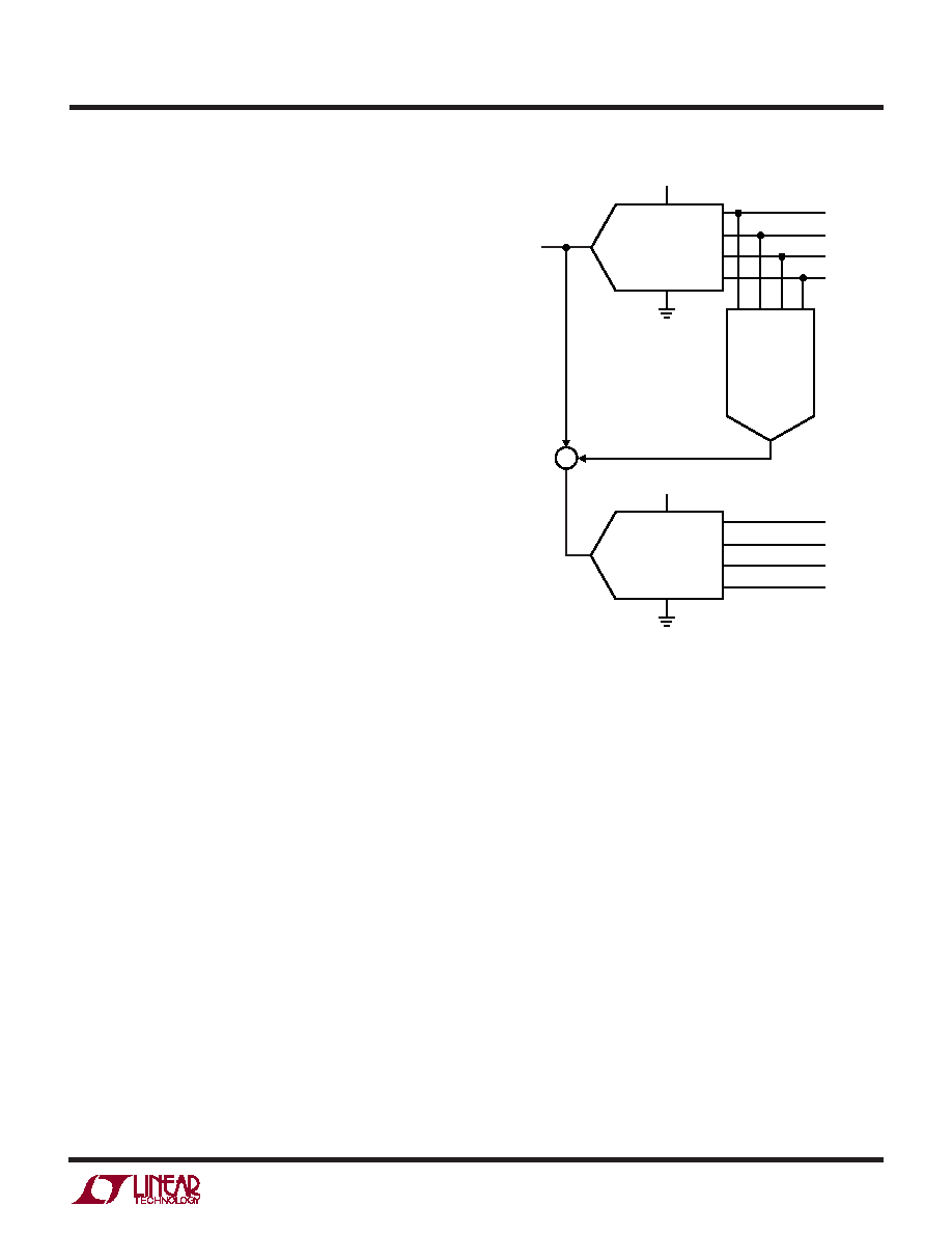
Figure 5 shows the functional block diagram for the
LTC1099 2-step flash ADC. It consists of two 4-bit flash
converters, a 4-bit DAC and a differencing circuit. The
conversion process proceeds as follows:
1. At the start of the conversion, the on-board sample-
and-hold switches from the sample to the hold mode.
This is a true sample-and-hold with an acquisition time
of 240ns, an aperture time of 110ns and a tracking rate
of 2.5V/
s.
2. The held input voltage is converted by the 4-bit MS-
Flash ADC. This generates the upper or most significant
4-bits of the 8-bit output.
3. A 4-bit approximation, from the DAC output, is sub-
tracted from the held input voltage.
4. The LS-Flash ADC converts the difference between the
held input voltage and the DAC approximation. This
generates the lower or least significant (LS) 4-bits of
the 8-bit output. The LS-Flash reference is one six-
teenth of the MS-Flash reference. This effectively mul-
tiplies the difference by 16.
5. Upon the completion of the LS 4-bit flash the eight
output latches are updated simultaneously. At the same
time, the sample-and-hold is switched from the hold
mode to the acquire mode in preparation for the next
conversion.
The advantage of this approach is the reduction in the
amount of hardware required. A full flash converter re-
quires 255 comparators while this approach requires only
31. The price paid for this reduction in hardware is an
increase in conversion time. A full flash converter requires
only one comparison cycle while this approach requires
two comparison cycles, hence 2-step flash.
This architecture is further simplified in the LTC1099 by
reusing the MS-Flash hardware to do the LS-Flash. This
reduces the number of comparators from 31 to 16. This is
possible because the MS and LS conversions are done at
different times.
To take the simple block diagram of Figure 5 and reconfigure
it to reuse the MS-Flash to do the LS-Flash is conceptually
simple, but from a hardware point of view is not practical.
A new six input switched capacitor comparator is used to
∑
+
–
LS
4-BIT
FLASH
MS
4-BIT
FLASH
4-BIT
DAC
VREF/16
VIN
VREF
B7
B6
B5
B4
B3
B2
B1
B0
1099 F05
REMAINDER
accomplish this function in a simple, although not straight
forward, manner.
Figure 6 shows the six input switched capacitor compara-
tor. Intuitively, the comparator is easy to understand by
noting that the common connection between the two input
capacitors, C1 and C2, acts like a virtual ground. In
operational amplifier circuits, current is summed at the
virtual ground node. Input voltage is converted to current
by the input resistors. In the switched capacitor compara-
tor, input voltage is converted to charge by the input
capacitors and these charges are summed at the virtual
ground node.
A major advantage of this technique is that the switch-on
impedance has no affect on accuracy as long as sufficient
time exists to fully charge and discharge the capacitors.
During the first time period the T+ and TZ switches are
closed. This forces the common node between C1 and C2
to an arbitrary bias voltage. Since the capacitors subtract
out this voltage, it may be considered, for the sake of this
discussion, to be exactly zero (i.e., virtual ground). Note
Figure 5. 8-Bit 2-Step Semiflash A/D
发布紧急采购,3分钟左右您将得到回复。
相关PDF资料
LTC1197IMS8#PBF
IC ADC 10BIT 500KHZ SHTDWN 8MSOP
LTC1198-1BCS8#PBF
IC ADC 8BIT 750KHZ SAMPL 8-SOIC
LTC1257IS8#TRPBF
IC D/A CONV 12BIT VOLT OUT 8SOIC
LTC1276ACN#PBF
IC A/D CONV 12BIT SAMPLING 24DIP
LTC1278-4IN#PBF
IC A/DCONV SAMPLNG W/SHTDN 24DIP
LTC1279CG#TRPBF
IC A/DCONV SAMPLNG W/SHTDN24SSOP
LTC1282ACN#PBF
IC A/D CONV SAMPLING W/REF 24DIP
LTC1288IS8#TRPBF
IC A/D CONV SAMPLING 12BIT 8SOIC
相关代理商/技术参数
LTC1099AI
制造商:LINER 制造商全称:Linear Technology 功能描述:High Speed 8-Bit A/D Converter with Built-In Sample-and-Hold
LTC1099AIJ
制造商:LINER 制造商全称:Linear Technology 功能描述:High Speed 8-Bit A/D Converter with Built-In Sample-and-Hold
LTC1099AIN
功能描述:IC A/D CONV 8BIT HI-SPEED 20-DIP RoHS:否 类别:集成电路 (IC) >> 数据采集 - 模数转换器 系列:- 标准包装:1,000 系列:- 位数:12 采样率(每秒):300k 数据接口:并联 转换器数目:1 功率耗散(最大):75mW 电压电源:单电源 工作温度:0°C ~ 70°C 安装类型:表面贴装 封装/外壳:24-SOIC(0.295",7.50mm 宽) 供应商设备封装:24-SOIC 包装:带卷 (TR) 输入数目和类型:1 个单端,单极;1 个单端,双极
LTC1099AIN#PBF
功能描述:IC A/D CONV 8BIT HI-SPEED 20-DIP RoHS:是 类别:集成电路 (IC) >> 数据采集 - 模数转换器 系列:- 标准包装:1,000 系列:- 位数:12 采样率(每秒):300k 数据接口:并联 转换器数目:1 功率耗散(最大):75mW 电压电源:单电源 工作温度:0°C ~ 70°C 安装类型:表面贴装 封装/外壳:24-SOIC(0.295",7.50mm 宽) 供应商设备封装:24-SOIC 包装:带卷 (TR) 输入数目和类型:1 个单端,单极;1 个单端,双极
LTC1099AM
制造商:LINER 制造商全称:Linear Technology 功能描述:High Speed 8-Bit A/D Converter with Built-In Sample-and-Hold
LTC1099AMJ
制造商:Linear Technology 功能描述:ADC Single Semiflash 400ksps 8-bit Parallel 20-Pin CDIP
LTC1099C
制造商:LINER 制造商全称:Linear Technology 功能描述:High Speed 8-Bit A/D Converter with Built-In Sample-and-Hold
LTC1099CJ
制造商:LINER 制造商全称:Linear Technology 功能描述:High Speed 8-Bit A/D Converter with Built-In Sample-and-Hold